这份文档是 pcb 程序的一个教程, pcb 是一个交互式印刷电路板(PCB)布局设计系统。
pcb 包含一个独立的程序(叫做 pcb ),它能让你创建、编辑和处理印刷电路板(PCB)的布局,同时也包含一个含有常用元器件的焊接外形(footprint)的库。
虽然当初这个程序是为Atari编写的(后来也运行于类Unix系统上),它已经被移植到了各种不同的平台上,包括Linux、Mac OS X和Windows。
虽然 pcb 可以以手动添加导线和元器件的方式单独使用,它只有在和电路图(schematics)编辑器如 gschem (一个源自 gEDA 项目的电路图编辑器,
能够生成网表(netlist)以保证元器件被正确连接等)一同使用的时候才会取得最佳效果。
pcb 储存数据用的文件以后缀名 .pcb 结尾,例如 myboard.pcb 。另外, pcb 从以后缀名 .fp 结尾的文件中
读取分立的元器件的印记(footprint),并从以后缀名 .net 结尾的文件中读取网表(netlist)。
pcb 支持很多种不同的输出格式。如果你需要用专业的制造技术来印刷你的电路板,你可以把你的电路板布局图导出成一个 RS-247X (也叫 gerber) 文件。如果你将要自己制造印刷电路板,
你可能会需要把布局图打印出来。你也可以把印刷电路板布局导出成PostScript封装的矢量图或者普通的图像文件(如PNG)以便在文档或者网页中使用。
关于格式的一点说明:在本文档中,“ pcb ”指的是整个pcb软件包,“ pcb ”指的是单独的程序,“ pcb ”或“ PCB ”指的是普通的印刷电路板。
各种EDA软件包中使用到的术语可能各有差异。为了更好的理解这份关于 pcb 的文档,认真阅读这些术语的定义是非常重要的, 它们能帮助你了解 pcb 将如何使用这些术语。
pcb 的命令都使用一个内部的通用接口来和GUI、脚本和用户的指令交互。我们把这些内部的通用接口叫做“ actions ”,
因为这些实际上是pcb可以直接执行的动作。根据每个“ action ”的有关文档,你可能需要给他们提供一些参数。“ actions ”被编写得跟函数调用一样,
如果你需要的话可以在 pcb 里按下“ : ”键来直接调用它们(跟 vi 类似的风格——译者注)。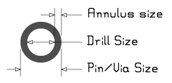
pcb 中,
一个“属性”是一个直接被传递给核心和各种 HID (如复选框和文件名)的关联。pcb 中一个用于存储临时数据并供以后使用的内存区域。其中一个缓冲区被用于执行普通的复制粘贴操作。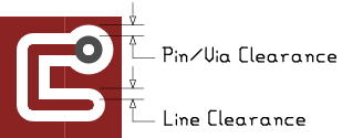
pcb 最多可以为同一个电路板生成两份不同的钻孔文件,
其中一个被用于金属化钻孔( plated holes),另一个被用于非金属化钻孔( unplated holes )。
自动钻孔机最初是由 Excellon 公司(参见版权声明)设计的,所以钻孔文件有时候也被叫做“ excellon ”文件。
它也可以被叫做“ NC drill ”文件。
gschem 电路图编辑器,它将生成 pcb 所能使用的的输入文件。pcb 可以使用的人机交互方式。pcb 使用相对于板子起始位置(即左上角)的坐标系统。但是,你可以设定电路板( board )上的原点以便 pcb 按此给出相对坐标。
这个位置就叫一个标记,它被用X形显示出来。元器件( Elements )也含有一个标记,这个标记是元器件( element )内部的坐标参考点。
元器件( Element )标记以小菱形给出。

pcb 会以有实际意义的方式在屏幕上显示这些层(即转换为正层显示——译者注),但导出程序可能会按制造单位的要求导出负片。pcb 作为输入数据的,它代表了电路板上电路的正确连接方式。
pcb 可以比较用户期望的(被程序载入的)网表和实际的(覆铜层上的)网表并为你指出短路或布线尚未完成的地方。如果有尚未完成连接的地方,
它可以利用那些网表信息为你建立一个临时网络( rat's nest )来帮助你完成布线。pcb 用以储存电路板布局的文件。这些文件以 .pcb 结尾并且可以作为纯文本文件进行读取和处理。pcb 用一个自己特有的单位来进行各种测量,这个单位比密尔( mils )和毫米都要小。
这也是 pcb 文件中使用的默认单位。在原作者(参见版权声明)撰写本文时,
pcb 单位是1/100密尔( mil ),或者10-5英尺。
pcb 中有一个单独的层来描述它。
在比较专业的制造车间( fabs )中每个层都会对应一个 gerber 文件。
pcb 的功能使用临时连接来确定要处理哪些联系,
所以在使用这些功能前更新临时布线很重要。pcb 中显示出来的阻焊剂层画出了阻焊剂存在的地方,
输出文件如 PostScript 或者 gerber 中,通常画出来的部分是要移去阻焊剂的地方。
参见负片( negative plane )——译者注。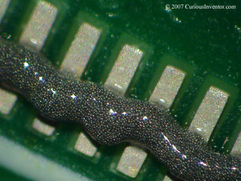


pcb 的GUI提供的一种绘图模式,在这种模式中物体都被绘制成细线(或轮廓)而不是有实际宽度的线条。这个模式在做细节调整工作的时候很有用,
因为它可以避免细小的物体的大小让它们之间的关系变得模糊。apt-get install pcb
emerge pcb
参见 ftp://ftp.netbsd.org/pub/NetBSD/packages/pkgsrc/cad/pcb/README.html。
apt-get install pcb pcb-gtk
在此章节,我们将会带领你制作一些简单的电路板,以便给你一个关于此程序如何工作的大致了解,并了解大多数项目都要做的一些共同的工作。每块板子都建立在前面一块板子中学习到的技术基础之上。
虽然这份文档并没有被写成一份 gschem 程序的教程,我们还是会指导你使用 gschem 的一些基本功能以便让你能够将其与 pcb 一同使用。如果需要更多的信息,
请您参阅 gschem 的文档(可以在 http://geda.seul.org/wiki/#faqs_quick_reference 找到——译者注)。
你将要做的第一块电路板简单到只包含一只发光二极管(LED)和一只电阻。它会让你看到该如何创建一块电路板,在上面放置元器件以及如何在上面走线。你将要做的第二块电路板是一只简单的闪烁灯, 它将需要制作电路图,创建工程文件以及创建新的元器件和印记。你将要做的第三块板子是另一个闪烁灯,这回它会使用表面安装工艺并且会有4个层,它们会引入供电用的平面、连接通孔以及阻热连接。
你的第一块电路板会让你了解 pcb 的基本操作。每一条首次引入的命令或操作都会被详细地解释一遍,但是随后就不会这样解释了。很多操作都能通过菜单或者键盘操作实现,
例如用 File→Quit Program 来选择“ File ”菜单中的“ Quit ”选项,或者直接使用快捷键 Ctrl-Q 。当我们提及 Ctrl-Q 时,
我们的意思是按住 <Ctrl> 键然后再按下 <Q> 键。当我们提及 Shift-Q 时我们指的是按下左右 <Shift> 键中的一个然后再按下 <Q> 键。
举个例子,当我们第一次描述“退出( Quit )”命令时, 我们会说:“现在使用‘退出( Quit )’命令( File→Quit 或者 Ctrl-Q ),来退出 pcb ”,
然后再次提及的时候我们只会说:“现在退出。”
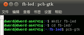
这个工程中的第一步是运行 pcb 程序。因为 pcb 默认使用当前目录作为它存放文件的工作目录,为这个工程创建一个子文件夹会是一个好主意,
cd 到这个文件夹里面,然后在终端模拟器中键入命令“pcb”或者“pcb-gtk”来运行它。
现在是练习“退出( Quit )”命令的一个好机会 :-)
另外,如果你向别人询问有关 pcb 的问题以寻求帮助,他们可能会需要知道你使用的是哪个版本和图形界面前端( GUI )。
你可以用“关于( About )”命令( Window→About... )来获取这些信息。
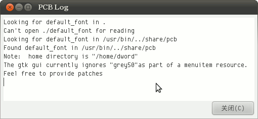
需要注意的是,当 pcb 启动时,它不仅仅还是创建了一个主窗口(如上图所示),它还会创建另外两个窗口。其中一个的标题是“PCB Library”,我们稍后会谈到它;
另外一个的标题是“PCB Log”,它包含了所有的消息——警告和错误等等。就现在而言,你大可以把它们挪开。如果你把它们关掉了,
你也可以用 Window→Library 和 Window→Message Log 把它们重新打开。
对于你创建的任何一块电路板来说,你所做的第一件事就包括决定电路板的大小有多大。如果你想把它做得尽可能地小,在创建它时你可以先把尺寸选得大一些,稍后再依据需要将其调小。 对于这块示例电路板,我们可以估计一下——我们想让它有一英寸(2.54厘米)见方的大小。电路板的尺寸有关选项在“ Preferences ”窗口里( File→Preferences ), 它包含一些与电路板和用户喜好有关的选项。我们需要修改板子的大小,所以单击“ Sizes ”选项。现在窗口看起来应该像这样:
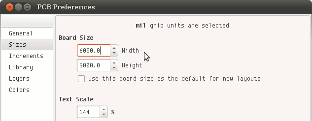
我们现在还用不到“ Text Scale ”(文本大小)和“ DRC ”(设计规则检查)。要注意的是这些数值的单位是密尔,所以默认的电路板大小是6英寸宽,5英寸高。
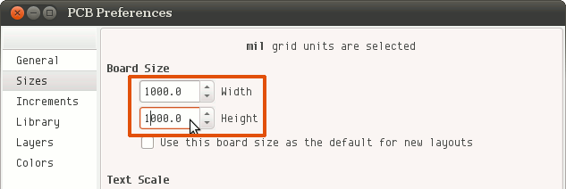
把这些数值全部改成 1000.0 :
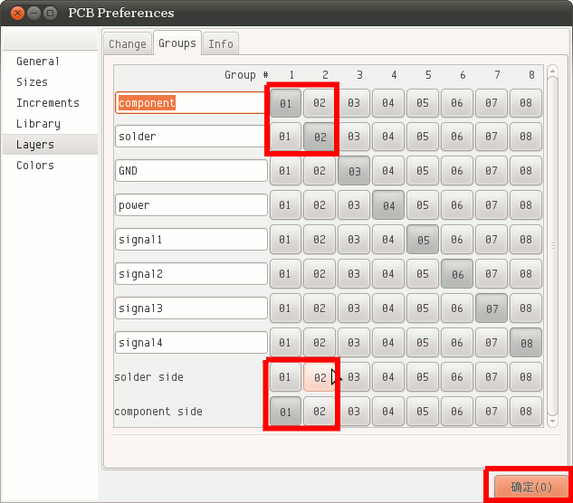
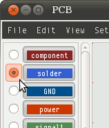
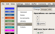
接下来我们会设置我们要用到的层,它决定了我们会有多少个覆铜层以及它们叫什么名字。选择“ Layers ”选项。你应该会在窗口顶部看到三个选项卡,单击“ Groups ”以便进入层组的设置。 对于这个工程来说,我们要确保的只是“ solder ”层与“ solder side ”(焊接面)一组并且“ component ”层与“ component side ”(元器件安装面)一组。 在按钮上单击以便把“ component ”和“ component side ”置于“ Group # 1”中,把“ solder ”和“ solder side ”置于“ Group # 2 ”中,然后单击“ 确定 ”。
还有一些你可能需要更改的选项,它们会随电路板布局被一同保存。首先,让我们打开可视的格点(单击 View→Enable visible grid ,如果它没被选中的话), 并且将网格间距设为0.1英寸——即100密尔( View→Grid Size→100 mil )。格点会被显示成一个小点组成的阵列,它们在显示出来的布局上可能很难被看到, 但是如果想办法让他们增多你就会很容易地观察到它们。你可以尝试把网格间距改成“ 10 mil ”来观察二者的区别(别忘了再改回来)。
下面,我们要确保我们走的线不会跟我们添加的多边形——例如大面积的地或者“ flood fill (填充区域)”——相连接。 Settings 菜单下面有很多设置, 但是现在你只要确保“ New lines, arcs clear polygons ”和“ Crosshair snaps to pins and pads ”处于被勾选的状态, 并且“ Auto enforce DRC clearance ”没有被选中就行了。
我们已经完成了电路板的基本设置,现在保存它是一个明智之举。使用“ Save ”(保存)命令( File→Save layout )。因为这是你第一次保存这个文件,
它会询问你电路板布局文件的文件名。我们会把这个文件命名为“ fb-led.pcb ”,所以在“ 名称 ”一栏中填入这个名字然后单击“ 确定 ”。
现在你的电路板就有一个与之相关联的文件了。你可以随时单击“ File→Save layout ”来保存你的劳动成果 :-)
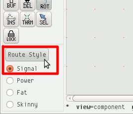
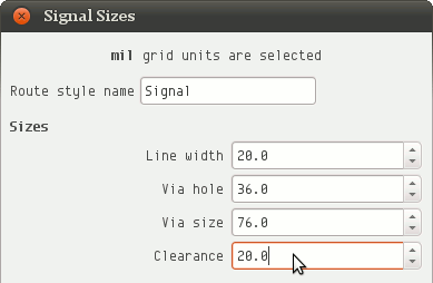
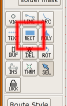
现在我们要往它上面添加实际的电路了。这个电路只是一个简单的LED、限流电阻以及接驳电池盒用的排针的串联电路。此例中我们不需要电路图,我们仅仅需要添加元器件然后手动把它们连接起来。 第一步是为你的布线选择一个“ route style ”(布线风格)。主窗口的左下角列举了4种可用的布线风格。确保“ Signal ”(信号线风格)被选中, 然后单击“ Route Style ”来打开布线风格编辑窗口。我们会把线条弄得粗犷些——这在简单的板子上很常见。在编辑窗口中,把“ Line width ”(线宽)设为20, “ Via hole ”(通孔直径)设为36,“ Via size ”(通孔大小——注意孔环)设为76,“ Clearance ”(间隙)设为20,然后单击“ 确认 ”。
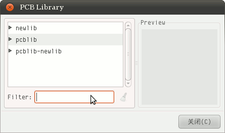
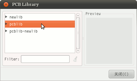
下面我们会添加三个要用到的元器件。在大一些的工程中,这个工作往往是由 gsch2pcb 完成的,不过你需要知道元器件的印记的名称。找到库(Library)窗口,如果它还开着。
如果你把它关上了,执行 Window→Library 来打开它。单击“ pcblib ”左侧的小三角来展开“pcblib”库。向下滚动,找到“ ~geda ”并单击它来展开“ ~geda ”集合。
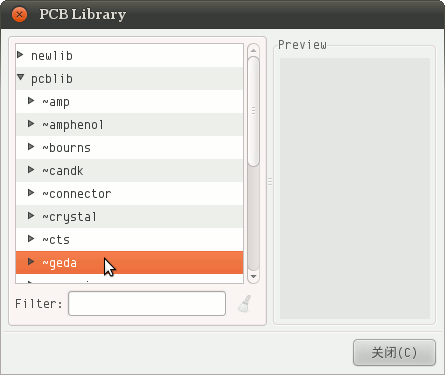
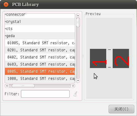
当你在库中选择了一个零件,你应该会注意到它的名称里面有个方括号——方括号里面就是你要在 gsch2pcb 中使用的印记名称。我们第一个要添加的元器件是LED。
我们会使用 RCY100P 印记来代表LED,这个印记是圆形的,有极性,间距为100密尔。向下滚动直到你找到它,
然后单击它(在较新的 pcb 中,你应该能在右侧的“ Preview ”中看到这个印记的预览——译者注)。当你把鼠标指针移回 pcb 主窗口中时,
你会发现鼠标指针带着所选元器件印记的轮廓:
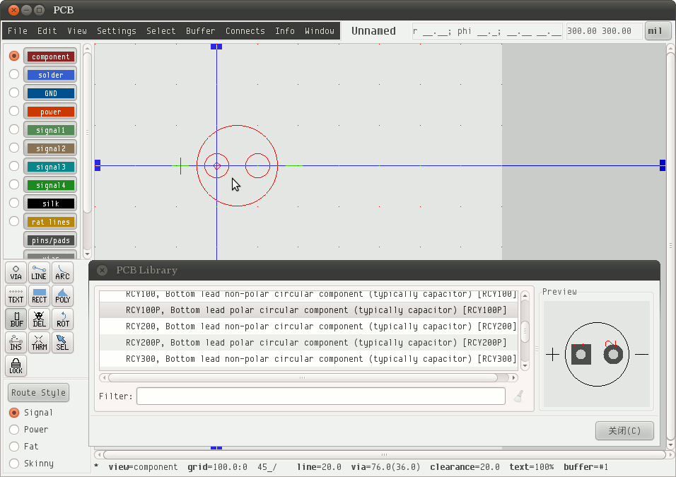
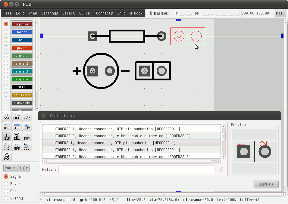
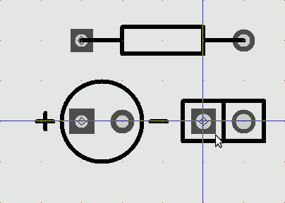
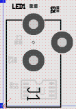
按下鼠标左键将元器件放置在你的电路板上。我们稍后会移动它。以此类推,把电阻用的 ACY400 印记和 HEADER2_1 印记也添加到板子上。
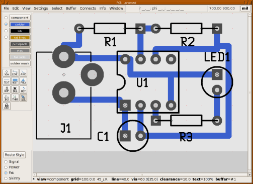
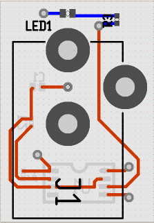
你的电路板现在看起来应该跟这个差不多:
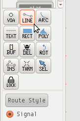
我们会使用选择( SEL )和旋转( ROT )工具来把各个元器件放到我们想要的位置。工具箱就在“布线风格”( Route Style )的上面,同样位于左侧工具栏中:
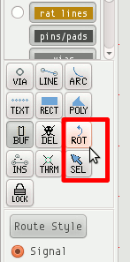
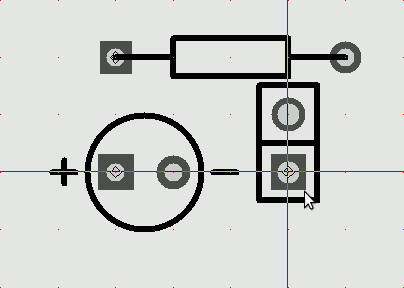
首先单击 ROT (旋转)工具。鼠标指针应该会变成一个图标来提示你点击任何东西它都会被旋转。把鼠标指针移动到排针的方形焊孔上,并单击鼠标左键:
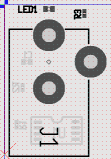
现在单击 SEL (选择)工具,也被称为“箭头工具”。当鼠标指针位于元器件上方时按住鼠标左键并移动鼠标可以移动它。元器件本身并没有动, 取而代之的是一个元器件的线条轮廓在移动(就像你在放置器件时的那样)。当你松开鼠标左键时,元器件本身会被移动到其轮廓被移动到的地方。
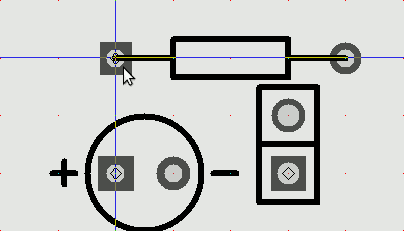
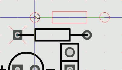
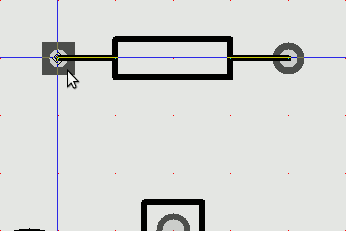
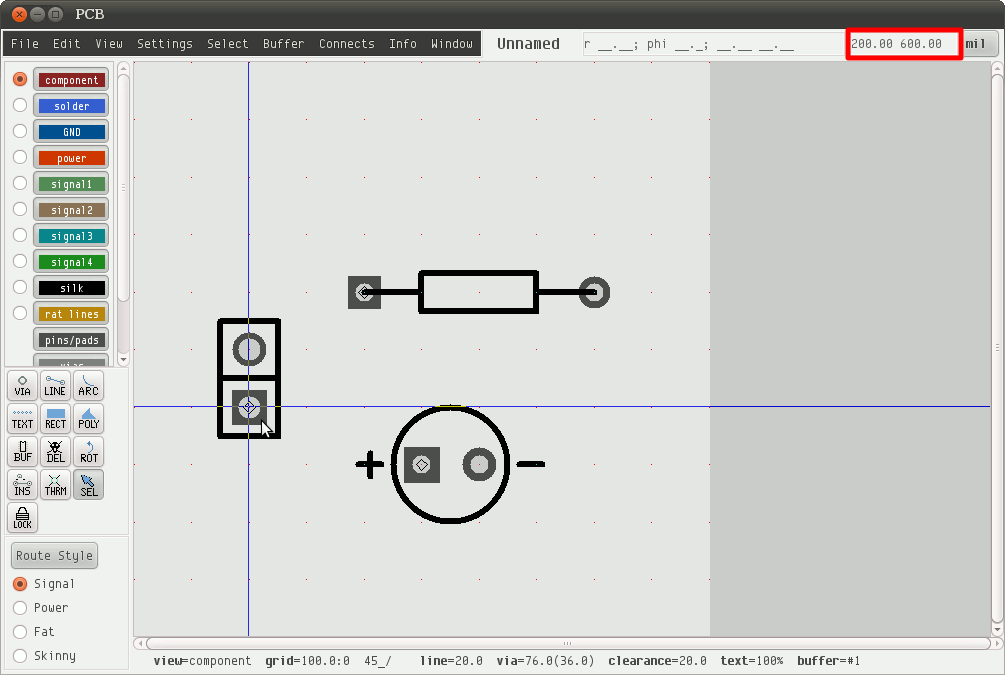
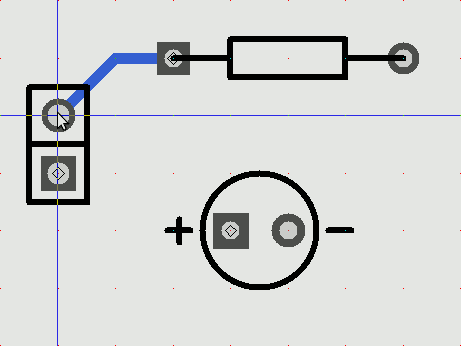
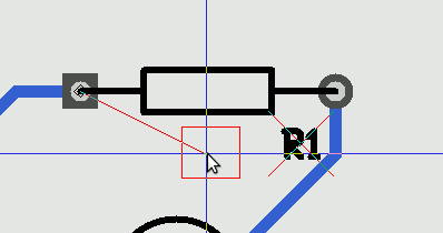
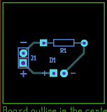
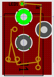
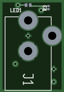
把排针的方形针脚移动到坐标200,600处(瞄准线的坐标会在主窗口右上角的状态栏里面显示出来,如下图红框所示),并且把电阻的方形针脚移动到400,400的位置。 最后把LED的方形针脚移动到500,700的位置。现在你的电路板看起来应该跟下面的一样:
现在你最好保存一下。
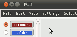
下一步我们会在元器件之间添加连接它们的布线。我们会用到 LINE (线条)工具来添加它们。因为这块板子比较简单,我们很有可能会把它弄成一个单面的电路板,线会被布在“背面”, 所以我们会把“ solder ”作为图层在其上布线。在主窗口左侧有一系列的以板子上各个层的名字命名的按钮,其中一个的名字是“ solder ”。在那个按钮的左边是一个小单选按钮, 单击它。不要单击按钮本身——这会改变层的可见性,即隐藏/显示层。单击单选按钮才会在层与层之间切换。
线条工具是这样是用的:首先你在线条开始的地方单击,然后移动瞄准线到线条结束的地方,最后再单击。由于它不需要你一直按住鼠标左键, 你可以卷动整块板子(按住鼠标邮件并移动——译者注)或者缩放(使用鼠标滚轮——译者注)来查找线条要终止的地方。你也可以在整个折线的各个顶点处单击来创建一条你想要的折线。 如果你要结束一条布线或者需要从别的地方开始一条新的布线,按下 Esc 键。如果你再按一次 键,你就会回到选择工具上。
如果你试图连接两个不在同一水平、垂直位置或是同一条对角线上的点,线条工具会创建一对布线来连接它们。其中的一条是水平或者垂直的,另外一调沿着对角线方向。
水平或者垂直的那段会连接着布线的起始点,而对角线方向上的那段会跟随着瞄准线。如果你观察一下主窗口底部的状态栏,你会看到一个“ _/ ”样的符号,标识着如下的信息:

按下键会改变这种模式。如果那个符号变成“ \_ ”,那么对角线方向上的那段会连接布线的起始端点,而水平或垂直的那段会跟随瞄准线移动,与刚才正好相反。
如果那里什么都没有的话(你可以多按几次 / ,同时观察状态栏——译者注),每次线条工具只会绘制一条直线段而不是两段。
另外,你也可以用 Shift 键(布线时先按住再移动——译者注)来临时地在“ \_ ”模式和“ _/ ”模式中间切换。
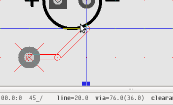
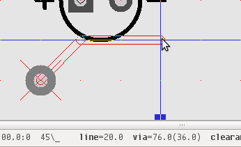
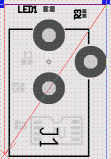
_/ ”模式(前)、“ \_ ”模式(中)和单段模式(后)——译者注。现在让我们添加所需的三条布线。按几下 / 键,把线条的分段模式调成“ _/ ”(这是 pcb 启动时的默认值),然后把电阻左侧的针脚与排针上侧的针脚连接。
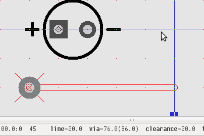
单击,移动,再单击,然后按下 Esc 。接下来把LED左侧的针脚与排针下侧的针脚连接起来。最后把电阻右侧的针脚和LED右侧的针脚连接起来。
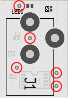
下面我们会对我们的PCB做一些调整。除非你使用了自己专门制作的库,你可能会需要在板子上再做一点小的调整。例如,你可能需要在两个针脚中间腾出空间以便让布线从其中穿过。就这块板子而言, 我们会做一些调整以便让它更适合在家制造。我们会把焊盘做得更大,以免我们钻孔时钻歪了。键盘上的 S 键对应着一个对任何物体都有效的改变大小命令。 把瞄准线移动到针脚上方然后按下 S 键,针脚的焊盘就会变得更大。如果你按了 Shift-S 针脚的焊盘就会变得更小。你可以这样改变针脚、焊盘、布线甚至丝印的大小。 但是,如果你想一次改变多个对象的大小,有一个更简单的办法。用 Select→Select all visible objects 菜单项来选择所有的对象。 现在你可以用 Select→Change size of selected objects 菜单项来调整所有所选对象的大小。对于此例, 我们希望使用“ Pins +10 mil ”选项来使我们的针脚焊盘变得更大一点(10密尔)。单击它之后,你会发现所有的针脚都变大了一点。 现在你可以用 Select→Unselect all objects 命令来取消选择所有的东西。
你也可以用选择工具( SEL )来进行选择和取消选择。你可以在要选择的器件上左键单击或者用鼠标拖动绘制出一个矩形来选定你想要选择的对象。如果要取消选择,在空白处单击一下就行了。 你也可以在按住 Shift 键来连续单击并选定多个不在一起的对象。
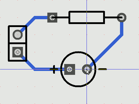
接下来我们会给各个元器件添加标签。每个元器件有三个可见的字符串,你可以通过 View 菜单中的选项来选择它们中的一个。默认情况下元器件的标识号(“reference designator”, 往往被简写成“refdes”)会被显示出来,这也是我们现在需要的。
由于针脚和元器件都可以添加标签,我们需要把网格关掉( View→Grid size→No Grid ),这样我们就可以选择元器件本身了。
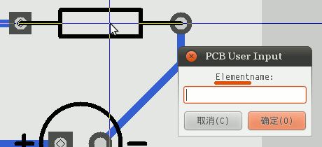
现在单击 Edit→Edit name of→text on layout 菜单项。这时界面的大部分会“变灰”,并且 pcb 会提示你 Select an Object (选择一个对象)。
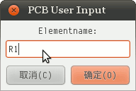
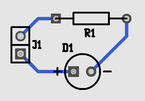
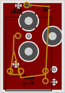
左键单击电阻本身,注意不要点在针脚上了。现在你应该可以看到一个弹出的对话框让你输入电阻的名称。你需要确认它提到了“ Element ”而不是“ Pin ”,然后键入 R1 并单击确认。
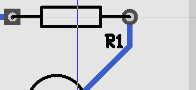
R1 (中)和最终的结果(后)——译者注。你可以到处拖动这个名称,但是小心不要错误地把布线也拖动了。
你也可以使用键盘快捷键来添加名称标签。将瞄准线对准 LED(注意不要对成针脚了),然后在键盘上按下 n 键(“ name ”的首字母),那个输入名称的对话框就会出现。
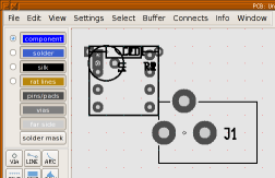
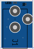
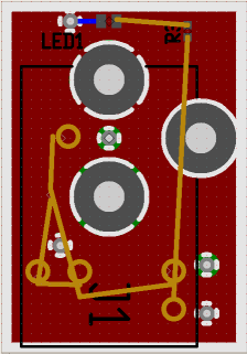
键入 D1 。然后将排针的名字改成 J1 并且稍稍调整标签的位置,直到它们看起来像这样:
不要忘了时不时地保存一下你的劳动成果。 一般情况下 pcb 每隔一段时间会自动保存一个副本,但是在适当的时候手动保存是一个好习惯。
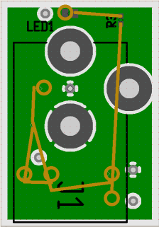
我们也可以在丝印层或者覆铜层添加额外的文本。现在让我们在排针旁边添加些说明性的文字,免得我们将电池插反。我们会使用到文本( text )工具:
We also want the silkscreen layer to be the default drawing layer:
Now, click below the header's square pin, and enter + in the
dialog that pops up. Use the S key a whole bunch of times to
make it bigger, then use the selection tool to move it in place. Do
the same for the - label.


Now that we're done with the labels, set the grid back to 100 mil in case you move any of the traces or parts; once they're off-grid it's hard to get them back on to the grid.
We're done editing the board now, so if you haven't already, save your work. But now that the board is done, what do we do with it? Well, that depends on how you're going to make your board. If you want to do it yourself, you probably want to send it to your printer. If you want someone else to make it, they'll probably want gerber files.
In your File menu, there are three options we're interested in.
The Print Layout... option prints your layout, but note that it will print 11 pages of board layers! This probably isn't what you normally want, but let's do it anyway.
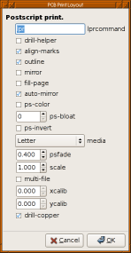
There are a lot of options there, but there's only a couple you need to worry about right now. Select fill-page and ps-color and click OK. Fill-page zooms your prints to fill the page. PS-color causes each layer to be printed in the same color as you see on the screen. If you're making boards at home using toner transfer, you want these options off, and you want mirror on.
In most cases, you don't want to just print the whole design. Usually you'll use the Export Layout... option to export your layout in a format that others can use. When you export, a list of possible export types is offered:
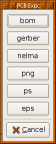
Click on gerber so we can create some Gerber (RS-274X) files, which are industry standard file for describing circuit boards.
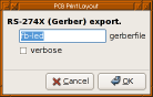
Click on verbose then OK. You'll see something like this in your terminal:
     Gerber: 5 apertures in fb-led.front.gbr
     Gerber: 5 apertures in fb-led.back.gbr
     Gerber: 3 apertures in fb-led.frontmask.gbr
     Gerber: 3 apertures in fb-led.backmask.gbr
     Gerber: 2 apertures in fb-led.plated-drill.cnc
     Gerber: 3 apertures in fb-led.frontsilk.gbr
     Gerber: 3 apertures in fb-led.fab.gbr
For a single sided board, most fab houses will need the back,
backmask, plated-drill, frontsilk, and fab files. pcb always
produces positive gerbers in case the fab asks.
For home fabrication, you'll want to print (see above) without the ps-color or fill-page options. For this simple board, printer calibration is not needed. If you're drilling your own holes, you may want to select the drill helper option, which reduces the diameter of the holes in the copper wherever you're drilling to help you center the drill properly. If you use the ps exporter, selecting the multi-file option puts each layer in a separate file. That way, you can print only the layers you're interested in.
So let's see what we've produced. Exit from pcb with
File→Quit Program and find your terminal again. I use the free
programs gv and gerbv to view my exported files;
gv is GhostScript, but your desktop probably knows what to do
if you double click on a .ps file in your file browser. gerbv
is a gerber file viewer that's part of gEDA:
$ gerbv fb-led.*.gbr fb-led.*.cnc
That's it! The next step is to actually make board (or have them made), which is beyond the scope of this tutorial.
This next board will introduce some additional concepts in pcb
that will help you with more complex board. It is assumed that you've
gone through the previous board, and those concepts will not be
re-explained. This board will be another single-sided board, but with
additional components. We will use a schematic to describe the
circuit, create some custom symbols and footprints, and learn to use
the autorouter.
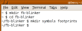
We will begin by creating our custom symbols and footprints. First,
we must create local symbols and footprint directories and teach the
tools to use them. My preference is to create subdirectories in the
project directory called symbols and footprints:
We then create some files to tell gschem and gsch2pcb to
look in these directories. The first is called gafrc and
contains just this one line:
(component-library "./symbols")
The second is called gschemrc and contains just this one line:
(component-library "./symbols")
The third is project-specific. The gsch2pcb program can read
its commands from a project file, and we will use this to tell it
about the footprints directory. The file is called
fb-blinker.prj and contains:
     elements-dir ./footprints
     schematics fb-blinker-sch.sch
     output-name fb-blinker
This project file tells gsch2pcb where to get element
descriptions, which schematics to read (we only have one), and what
base name to use for the various output files.
We must create two custom symbols for this project. The first is for
our power jack, and is a purely custom symbol. Creating such symbols
is beyond the scope of this tutorial. Please refer to the
gschem documentation for that. The second symbol uses the
djboxsym utility which you can download from the web (see
http://www.gedasymbols.org/user/dj_delorie/tools/djboxsym.html).
The first symbol is called symbols/powerjack.sym and looks like
this:
There's a copy of this symbol in the source distribution for this
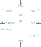
documentation. The second symbol is built from this 555.symdef
file:
     [labels]
     555
     refdes=U?

     [left]
     7 DISCH

     6 THRESH
     2 TRIG

     [right]
     4 RES

     3 OUT

     5 CTRL

     [top]
     8 VCC

     [bottom]

     1 GND
and looks like this:
Now, using those symbols, create your schematic, and name it fb-blinker-sch.sch. There's a copy of the schematic file in the source distribution also. It should look like this:
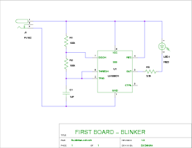
Using gschem and/or gattrib, set the footprint
and value attributes as follows:
| refdes | footprint | value
| |
| C1 | RCY100 | 1uF
| |
| J1 | pj-102.fp | PJ102
| |
| LED1 | RCY100 | RED
| |
| R1 | ACY400 | 100k
| |
| R2 | ACY400 | 100k
| |
| R3 | ACY400 | 3.3k
| |
| U1 | DIP8 | LM555CN
|
Now we must create the custom footprint for the power jack. While
there are various contributed tools that can be used for large
footprints (like BGAs), for small parts like this the easiest way is
to create the footprint in pcb itself. This is done by
creating a board with vias and lines, then converting it to an
element and saving it.
Change to the footprints subdirectory and start pcb. It
doesn't matter how big the working area is, or the layer stackup.
Looking at the specs for our power jack, we note that measurements are
given in tenths of a millimeter, so we'll use a metric grid. To
start, set the grid to 1mm, move the crosshairs to the center of
the board, and press Ctrl-M to set the mark. This will be the
reference point for all our measurements. By doing this with a large
grid value, we ensure that it will be easy to click on the same spot
later on if needed.
Now set the grid to 0.1mm, which we'll use to place all our vias and lines. We're using vias to create pins, so we need to set the via size and drill diameter. Click on the Route Style button to bring up the route styles dialog, and set Via hole to 1.6mm and Via size to 3.6mm. While we're here, set Line width to 0.15mm, we'll need that when we draw the outline later.
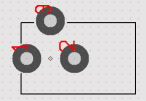
Now, zoom in enough to see the grid points. Place one via 3mm to the left of the mark, one 3mm to the right, and one 4.7mm above. Sequence is important! The pins will be numbered in the same order as the via creation. To place a via, select the Via tool, position the crosshair, and press the left mouse button.

Using the line tool, the same tool you used to draw copper traces in the first board, we will draw an outline of the jack on the silk layer. Select the line tool, and make the silk layer active. Draw as much of a box as you can which extends 10.7mm to the right of the mark, 3.7mm to the left, and 4.5mm above and below. Be careful not to draw on top of your pins, or your board will have ink on the pins. It should look something like this:
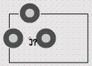
Now, set the grid back to 1mm so we can easily click on the mark. Select everything by using the Select→Select all visible objects menu button. Position the crosshair on the mark and press Ctrl-C to copy all the objects to the buffer. Use the Buffer→Convert buffer to element menu button to convert the buffer to an element. You can now click somewhere else on the board to paste a copy of your new element for inspection.
The first thing to do is check the pin numbers. Place the crosshair on the mark and press the D key to turn on the pin numbers. Check to make sure they're correct, then press D to turn them back off again.
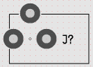
Now, we're going to set the default position of the label. Place the
crosshair on the mark and press the N key. Change the element
name to J?. By default it shows up at the element's mark. Use
the selection tool and S key to position the label as shown
below.
Using the selection tool, position the crosshair on the element's mark
and click on it to select it. Press Ctrl-C to copy it to the
buffer, and use Buffer→Save buffer elements to file to save your
new footprint to a file. Save it as pj-102.fp in the
footprints directory. Note that the name of the file must match the
footprint attribute you used for the power jack in your schematics.
Congratulations! You've created your first custom footprint.
Now that we have our schematics and custom footprint, we need to
figure out how to start the board layout. The tool we will use is
gsch2pcb, which reads schematics and can create or update a
board to match. Since gsch2pcb doesn't use the same defaults
as pcb, we will create the board in pcb and only use
gsch2pcb in update mode.
When creating a non-trivial board, it's a good idea to start with a
larger board than your final size. For this project, the final size
will be 1.4 inches wide by 0.9 inches high. However, we'll start with
2 by 2 inch board to give us some room to move things around. Run
pcb and create your board, setting up the size, layers, and
styles just like in the last project. Make sure you set a 100 mil
grid, since the parts we're using are all designed with 100 mil
spacing in mind. Also, make sure Settings→Crosshair snaps to
pins and pads is checked. Save this empty board as
fb-blinker.pcb and exit.
Now we run gsch2pcb, passing it the name of the project file:
     $ gsch2pcb fb-blinker.prj

     ---------------------------------
     gEDA/gnetlist pcbpins Backend
     This backend is EXPERIMENTAL
     Use at your own risk!
     ---------------------------------

     Using the m4 processor for pcb footprints

     ----------------------------------
     Done processing.  Work performed:
     1 file elements and 6 m4 elements added to fb-blinker.new.pcb.

     Next steps:
     1.  Run pcb on your file fb-blinker.pcb.
     2.  From within PCB, select "File -> Load layout data to paste buffer"
         and select fb-blinker.new.pcb to load the new footprints into your existing layout.
     3.  From within PCB, select "File -> Load netlist file" and select
         fb-blinker.net to load the updated netlist.

     4.  From within PCB, enter

                :ExecuteFile(fb-blinker.cmd)

         to update the pin names of all footprints.
What gsch2pcb does is remove elements from your board that don't exist in the schematic, provide new elements that need to be added, generate an updated netlist, and create a script that renames all the pins. You don't need to use all these - for example, I rarely use the pin renaming script - but we will this time, so you can learn how each file is used.
We will do as the hints above tell us to do. Run pcb
fb-blinker.pcb to bring up the empty board. Load the new element
data, which automatically changes you to the buffer tool. Click on
the board to place all those new parts. They'll all be in the same
place, but we'll fix that later. Load the new netlist, and run the
script. After closing any dialogs that may have come up, your board
should look like this:
The next step is to separate the elements so we can start laying out our board. Use the Select→Disperse all elements menu option, which spreads apart the elements. Then, use the Connect→Optimize rats nest menu option (or the O key) to draw all the rats on the board. These will help you figure out an optimum layout of your elements. Your board should look something like this (yours may vary depending on how the dispersal worked):
If you position the crosshair over U1 and press the D key, you'll see that the pins are now labelled with the same labels as in the schematic. You can use the View→Enable Pinout shows number menu checkbox to toggle between the symbolic labels and the original pin numbers.

Now, as before, we want to rearrange the elements to minimise and
simplify the connections. This is where the rats come in handy. As
you rearrange the elements, the rats follow, so you can see how
rotating and moving elements affect the layout. As you move elements
around, press the O key to tell pcb to figure out the
best way of connecting everything in their new locations.
As you move the elements around, remember to pick up the power jack by its mark, as the power jack's pins have metric spacing. The other elements should be picked up by their pins, since they have inch spacing. By picking up elements by their pins, you ensure that their pins end up on the grid points when you put them down.
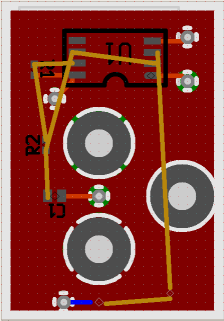
Rearrange your elements so that they look like this, somewhere near the center of your board. Note that the rats nest will tell you when you have the resistors backwards, since they don't have polarity like the LED or IC have.
As before, we want to move the refdes labels around so that they're both visible and out of the way. To make this easier, use the Settings→Only Names option to keep the tools from accidentally selecting elements or rat lines. Shut off the grid, and use the selection and rotate tools, and the S size key, to make the labels like this:
Now use Settings→Lock Names to keep from accidentally moving our labels later. We're still using our over-sized board. Now is the time to reduce it to the final size. First, we have to move the elements to the upper left corner of the board. Set the grid back to 100 mil, Select→Select all visible objects, grab one of the pins, and move everything up to the corner, as close as you can get without touching the edges:
Click to de-select and change the board size to 1400 mils wide by 900 mils high. Don't forget to save often!
Again, we're planning on hand-soldering this board, so select everything and make all the pins 10 mils bigger than the default.
Rather than route all the traces by hand, for this board we will use the autorouter. There are a few key things you need to keep in mind when using the autorouter. First, the autorouter will use all available layers, so we must disable the layers we don't want it to route on. To do this, click on the component button to disable that layer:

The autorouter also uses whatever the default style is, so select the Fat style:

The autorouter uses the rats nest to determine what connections will be autorouted, so press O now to make sure all the rats are present and reflect the latest position of the elements. To do the autorouting, simply select the Connects→Autoroute all rats menu option.
In theory, you could consider your board done now, but to make it look more professional, we will do two more steps. Use the Connects→Optimize routed tracks→Auto-Optimize menu option twice (or until no further changes happen) to clean up the traces left by the autorouter:
And finally, select Connects→Optimize routed tracks→Miter to miter the sharp corners:
Your board is done. As before, you can print your design or produce Gerber files, according to how you're going to have your board made.
The third and final board in the first board series will teach you about multi-layer boards, vias, and SMT components. Again, we assume you've done the other two boards, and will not re-explain concepts taught there. We will be using the same circuit as the last board, but to make things interesting, we will be adding some constraints. The board must be as small as possible, EMI-proof, and able to handle rework. Ok, I'm making this up, but what it means is that we will be using the smallest components a hobbyist can expect to use, a four-layer board, and more vias than would otherwise be needed. We do this to give us the opportunity to learn these techniques, without spending undue time due to an overly large schematic.
We begin with the same schematic as before. To assist us in assigning
power planes, we need to name the power rails in the schematic. See
the gschem documentation for details, but what you want is to
name the ground net GND and the power net Vdd. Set up a
new fb-smt.prj project file as before. Use gattrib to
set the footprint attributes as follows:
| refdes | footprint | value
| |
| C1 | 0402 | 1uF
| |
| J1 | pj-102.fp | PJ102
| |
| LED1 | 0402 | RED
| |
| R1 | 0201 | 100k
| |
| R2 | 0201 | 100k
| |
| R3 | 0201 | 3.3k
| |
| U1 | MSOP8 | LMC555CMM
|
Run pcb and set up your blank board. Put component and
component side in group 1. Put GND in group 2, power in
group 3, and solder and solder side in group 4. Switch to the
Change tab, select the solder layer in the main window, and
move the solder layer down under the power layer.
Set the board size to 50 mm by 50 mm. To set a metric size, use the
View→Grid units→mm menu option. Then, the Sizes
preference will use millimeters. Set the DRC values to 0.35 mm (about
13.5 mil) for drill and 0.15mm (about 6 mil) for everything else.
Save your board, exit pcb, and run gsch2pcb fb-smt.prj.
Go back to pcb, import and disperse the new elements, and load
the netlist.
As before, move the labels out of the way and size them accordingly. You should end up with something like this:
The final size of our board will be 12.5mm wide by 18 mm high, not much bigger than the power jack. Start by rotating the power jack to face down, and put its mark at 5.5mm by 7mm. The LED goes just above it, with R3 to the right of the LED. The rest of the elements will go on the other side of the board. Here's how:
For each element that needs to go on the other side of the board, place the crosshair over the element and press the B key
The element shows as a light gray because it's now on the far side of the board (Note that one of the layer buttons says far side on it). You can flip the board over (making the far side the near side, and visa-versa) by pressing the Tab key. Since the elements we need to place are on the far side, now, flip the board over. Note that this is an up-down flip, so the power jack now appears in the lower left corner instead of the upper left. There are other types of flips you can do by using Shift-Tab (left-right flip), Ctrl-Tab (180 degree rotation), or Ctrl-Shift-Tab (nothing moves, sort of an X-Ray view).
Anyway, move the remaining elements around so that they look like this:
When routing a multi-layer board, I find it best to start with the
power and ground planes. First, resize the board to be 12.5 mm wide
by 18 mm high, and flip it so you've viewing the component side (the
side with the power jack). If your version of pcb does not
permit sizes this small (some versions have a one inch minimum, others
0.6 inch), save the file, exit pcb, and edit fb-smt.pcb
in a text editor so that the PCB line looks like this:
PCB["" 49213 70866]
When you run pcb again, the board will have the right size.
Set your grid to 0.5 mm and make sure it's visible. There are two
ways to create a plane layer, which means a layer that's mostly
copper. Such layers are often used for power and ground planes. The
first way is to use the polygon tool; the second is to use the
rectangle tool, which is just a shortcut for the polygon tool.
Make the GND layer the current layer and select the POLY tool:
The polygon tool works by clicking on each corner of the polygon, in sequence. You complete the polygon by either clicking on your start point again, or by pressing Shift-P. We will create a polygon that's 0.5mm away from the board edge. In these images, we start at the lower left corner and work our way around clockwise. When we click on the lower left corner again, the polygon is created:
In this case, we're just drawing a rectangle, but if you need any other shape, just click on the corners as needed. As a shortcut, you can create a rectangle with the rectangle tool, which creates rectangle-shaped polygons. Make the power layer the current layer and select the RECT tool:
Like the polygon tool, the rectangle tool works by clicking on corners. However, you only have to click on two diagonally opposite corners, like this:
If the color difference is too subtle for you, you can choose other colors through the File→Preferences menu option. We will set the GND layer to green and the power layer to red for the remainder of this tutorial.
To connect the ground and power planes to their respective nets, we'll use a thermal to connect the power jack's pins to them. We could also just draw a line from the pin to the polygon, but thermals are better suited to this task. Select the THRM tool:
What the thermal tool does is connect (or disconnect) thermal fingers between pins or vias, and the polygons around them. Each time you click on a pin or via, the thermal fingers are connected to the current layer. We want to find the pin on the power jack that's connected to ground in the schematic, and connect it to ground on the board. We use the netlist dialog to do so. First, optimize the rats net with O and make the GND layer current. If the netlist dialog isn't shown, use Window→Netlist to show it. Select the GND net and click on Find:
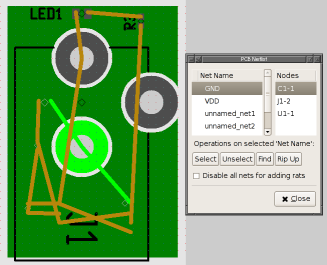
Notice that one of the pins on the power jack has been highlighted. That's the one that is supposed to be connected to the ground plane. Click on it to create a thermal:
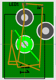
If you optimize the rats nest again, the rats won't connect to that pin any more, and the other pins and pads that need to connect to the ground plane are now marked with circles, meaning these need to be connected to a plane. Anyway, make the power plane the current plane, find the VDD net in the netlist and create its thermal on the found power jack pin. Note that the green GND thermal fingers on the other pin show through the gap in the red power plane - thermals are created on a specific layer, not on all layers.
If you tried to autoroute the board at this point, it would just connect all those power and ground pins to the power and ground pins on the power jack. So, we will first tie all the power and ground pins to their planes manually, using vias. We're doing this mostly to demonstrate how to do it, of course. The first step is to place the vias. Select the VIA tool from the left panel:

Click on the Route Style button to bring up the route styles dialog, and set Via hole to 0.4mm and Via size to 0.8mm. Also set Line width to 0.25mm. Create vias near the pins that are connected to the planes, as such:
Note that I've shut off the ground and power planes, as well as rat lines, to help you see where the vias should go. Shut off the GND plane and find the VDD net again, to highlight which rat circles (and thus their vias) need to connect to the power plane. Like you did with the power jack's pins, use the thermal tool to connect the relevent vias to the power plane. Repeat for the GND plane.
Now you have to connect the vias to the pins that need them. For the LED it's easy, that trace goes on the top. Make the component layer the current layer and use the LINE tool like you've done before to draw a line from the via next to the LED, to the pad on the LED that's connected to VDD. For the other connections, you'll want to flip the board over, so use the Tab key to flip the board over, make the solder layer the current layer, and connect the rest of the power/gnd pins to their vias. If you press O now, you'll see that all the rat-circles have gone away:
The last step is autorouting. Hide all the power, ground, and silk layers, optimize the rats nest (O), and run the autorouter, optimizer, and miterer. Done! Here's what the board looks like with the thin draw polygons setting checked, to only draw outlines for the power and ground planes, along with some photo-quality prints:
本文档的PDF版本(目前未翻译)请点 这里 下载。
与文档有关的电路图与印记文件可以在 这里 下载。
文档的源代码(目前未翻译)可以在 这里 下载。
版权声明:
“ Excellon ”是 Excellon Automation Co. 的注册商标。
“ Gerber ”是 Gerber Scientific, Inc. 的注册商标。
其他的商标归其所有者所有。
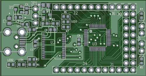
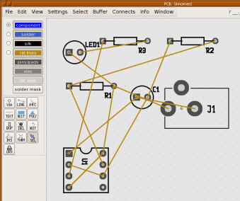
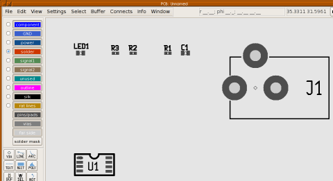
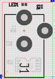
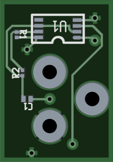
本文开头的示例图像源自原作者的USB GPIO Pod项目,参见http://www.delorie.com/electronics/usb-gpio/
锡膏的图像源自http://store.curiousinventor.com/guides/Surface_Mount_Soldering/Solder_Paste_and_Toaster_Oven/,版权归其所有。此图像为译者添加。
原文地址:http://www.delorie.com/pcb/docs/gs/
原文作者:DJ Delorie < >
>
翻 译:dword < >
>
授权协议:GNU 通用许可证